Difference between revisions of "IoT - ESP-Everything!"
| (25 intermediate revisions by the same user not shown) | |||
| Line 3: | Line 3: | ||
My personal response to the weirdness that is ESP module form factors. | My personal response to the weirdness that is ESP module form factors. | ||
| − | My introduction to ESP was the ESP-07. | + | My introduction to ESP was the [[ESP-07]]. |
It's an awesome module to play with. But it has a few issues. | It's an awesome module to play with. But it has a few issues. | ||
==The Issues== | ==The Issues== | ||
| − | '''Issue #1:''' ESP devices run on 3.3V, not the ubiquitous 5V you can easily get by grabbing the nearest spare phone charger. This one's pretty simple. Put a 3.3V regulator in there. (I tend to grab the AMS1117-3.3. Cheap & easy...) | + | '''Issue #1:''' ESP devices run on 3.3V, not the ubiquitous 5V you can easily get by grabbing the nearest spare phone charger. This one's pretty simple. Put a 3.3V regulator in there. (I tend to grab the [[:File:Ds1117.pdf|AMS1117]]-3.3. Cheap & easy...) |
| − | '''Issue #2:''' Every ''standard'' ESP module has a weird pinout at a weird pin pitch. Dunno why. They just do. Even the ESP-01 has a pain-in-the-ass pin layout. (but, at least it's on 0.1" spacing. Too bad it's designed to avoid breadboard compatibility...) | + | '''Issue #2:''' Every ''standard'' ESP module has a weird pinout at a weird pin pitch. Dunno why. They just do. Even the [[ESP-01]] has a pain-in-the-ass pin layout. (but, at least it's on 0.1" spacing. Too bad it's designed to avoid breadboard compatibility...) |
'''Issue #3:''' The most annoying one... To program an ESP chip, you have to hold gpio0 low during bootup or reset. Then you have to reset the board again to get out of programming mode. I get why they did it this way, but it's annoying. | '''Issue #3:''' The most annoying one... To program an ESP chip, you have to hold gpio0 low during bootup or reset. Then you have to reset the board again to get out of programming mode. I get why they did it this way, but it's annoying. | ||
| Line 27: | Line 27: | ||
==What I've done to try & solve a few of these issues== | ==What I've done to try & solve a few of these issues== | ||
| − | After discovering the ESP-M3, I determined that it would be nearly ideal for embedding into projects. | + | After discovering the [[ESP-M3]], I determined that it would be nearly ideal for embedding into projects. |
So I set out to design a carrier board for it. | So I set out to design a carrier board for it. | ||
| Line 38: | Line 38: | ||
**Make it hard to blow up with reverse power | **Make it hard to blow up with reverse power | ||
*Programming header | *Programming header | ||
| − | **Compatible with the typical Sonoff header would be good | + | **Compatible with the typical [[IoT - Sonoff|Sonoff]] header would be good |
**Capable of automatic mode selection | **Capable of automatic mode selection | ||
*Breakout '''ALL''' available gpio pins from the module | *Breakout '''ALL''' available gpio pins from the module | ||
| Line 54: | Line 54: | ||
*Input: | *Input: | ||
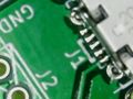
**Directly soldered USB-micro connector (J1) | **Directly soldered USB-micro connector (J1) | ||
| − | **My favourite USB breakout board (J2) J2 is basically positioned on the board such that using the breakout instead of soldering a connector directly to the board leaves the USB connector in the same spot, just 1.5 mm higher. | + | **My favourite USB breakout board (J2) J2 is basically positioned on the board such that using the breakout instead of soldering a connector directly to the board leaves the USB connector in the same spot, just 1.5 mm higher. |
| − | + | **Direct wiring (J2)<gallery> | |
| + | File:Molex USB Pins.jpg|Tiny little pins under the microscope. | ||
| + | File:Breakout-2.jpg|Preferred connector breakout | ||
| + | File:Breakout-1.jpg|Stronger connector breakout | ||
| + | File:Direct Wiring.jpg|Pin Header on J2 (or you could just solder wires in too...) | ||
| + | </gallery> | ||
*Reverse polarity protection (D1) | *Reverse polarity protection (D1) | ||
**Note: The (nearly invisible) stripe on the diode should be to the left when installed. (towards the D1 marker) | **Note: The (nearly invisible) stripe on the diode should be to the left when installed. (towards the D1 marker) | ||
| Line 63: | Line 68: | ||
*Indication (R2D2) :P | *Indication (R2D2) :P | ||
**When I initially put a power LED on board with its resistor, KiCAD generated the annotation... It went from there... | **When I initially put a power LED on board with its resistor, KiCAD generated the annotation... It went from there... | ||
| − | **Note: The cathode (- side) of D2 goes up. (towards R2D2s head) | + | **Note: The cathode (- side) of D2 goes up. (towards R2D2s head) Which puts the "T" shape on the bottom of the part upside-down... |
| + | |||
| + | =====Assembly & Testing===== | ||
| + | |||
| + | #J1 | ||
| + | #*Should have 5v at pin-1 of J2 if you connect to a USB source | ||
| + | #D1 | ||
| + | #*Diode test (common on U1 & + on Vcc) = 0.211v | ||
| + | #U1 | ||
| + | #*Should have +3v3 from ground to any 3v3 point on the board | ||
| + | #C1 | ||
| + | #*This tantalum cap should NOT explode if you connect a USB source :O | ||
| + | #R2D2 | ||
| + | #*D2 should light up if you connect a USB source | ||
====Programming==== | ====Programming==== | ||
| Line 76: | Line 94: | ||
*Automatic mode selection (Q1 & Q2) | *Automatic mode selection (Q1 & Q2) | ||
**This idea was shamelessly stolen from the D1-mini | **This idea was shamelessly stolen from the D1-mini | ||
| + | **For flashing from PlatformIO, add <code>upload_resetmethod = nodemcu</code> to your '''platformio.ini''' file | ||
| − | ===== Testing ===== | + | =====Testing===== |
Using a DMM in Diode-Mode, measure from RST to RTS & DTR. Then do the same from GPIO0. (by "from" & "to", I mean put the common lead of your meter on the "from" point & the positive lead on the "to" point...) | Using a DMM in Diode-Mode, measure from RST to RTS & DTR. Then do the same from GPIO0. (by "from" & "to", I mean put the common lead of your meter on the "from" point & the positive lead on the "to" point...) | ||
| − | * RST | + | *RST |
| − | ** RTS = 0. | + | **RTS ~= 0.8v |
| − | ** DTR = 0. | + | **DTR ~= 0.5v |
| − | * GPIO0 | + | *GPIO0 |
| − | ** RTS = 0. | + | **RTS ~= 0.5v |
| − | ** DTR = 0. | + | **DTR ~= 0.8v |
| + | |||
| + | The numbers might not be exact depending on how your meter does diode-mode. But here should be SOMETHING across those transistors. | ||
====I/O==== | ====I/O==== | ||
| Line 106: | Line 127: | ||
*All the empty space on the board... :P | *All the empty space on the board... :P | ||
| + | |||
| + | ====A little extra about the board designs==== | ||
| + | While designing these boards, it has come to my attention that some of the default footprints in KiCad truly suck for hand soldering. So I've put in the effort to learn how to edit footprints... | ||
| + | |||
| + | [[KiCAD - Tinkers Custom Footprints|Tinkers Custom Footprints]] | ||
| + | |||
| + | Also, sometimes you might just need to create your own symbol libraries... | ||
| + | |||
| + | [[KiCAD - Tinkers Custom Symbols|Tinkers Custom Symbols]] | ||
| + | |||
| + | Eventually I'll even learn to create my own parts in 3D for the 3D board view... | ||
| + | |||
| + | [[KiCAD - Tinkers Custom 3D Stuff|Tinkers Custom KiCad 3D Stuff]] | ||
===BOM=== | ===BOM=== | ||
| Line 128: | Line 162: | ||
**CRCW08054K70FKEA | **CRCW08054K70FKEA | ||
**[https://www.digikey.ca/en/products/detail/vishay-dale/CRCW08054K70FKEA/1175713 RES SMD 4.7K OHM 1% 1/8W 0805] | **[https://www.digikey.ca/en/products/detail/vishay-dale/CRCW08054K70FKEA/1175713 RES SMD 4.7K OHM 1% 1/8W 0805] | ||
| + | ***or | ||
| + | **CRCW08052K20FKEA | ||
| + | **[https://www.digikey.ca/en/products/detail/vishay-dale/CRCW08052K20FKEA/1175673 RES SMD 2.2K OHM 1% 1/8W 0805] | ||
*J1 | *J1 | ||
**Molex 1050170001 | **Molex 1050170001 | ||
| Line 144: | Line 181: | ||
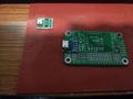
*[[IoT - ESP-M3 Everything!|ESP-M3 Everything!]] | *[[IoT - ESP-M3 Everything!|ESP-M3 Everything!]] | ||
**(The original board) | **(The original board) | ||
| − | |||
**'''Built AND Tested... Successfully!''' | **'''Built AND Tested... Successfully!''' | ||
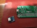
*[[IoT - ESP-01 Everything!|ESP-01 Everything!]] | *[[IoT - ESP-01 Everything!|ESP-01 Everything!]] | ||
*[[IoT - ESP-07 Everything!|ESP-07 Everything!]] | *[[IoT - ESP-07 Everything!|ESP-07 Everything!]] | ||
| − | ** | + | **'''Built AND Tested... (mostly) Successfully!''' |
| − | ** | + | **Board needs a respin... |
| + | *[[IoT - ESP-01F Everything!|ESP-01F Everything!]] | ||
| + | *[[IoT - ESP-12 Everything!|ESP-12 Everything!]] | ||
*[[IoT - ESP-?? Everything!|ESP-?? Everything!]] | *[[IoT - ESP-?? Everything!|ESP-?? Everything!]] | ||
**(The generic board) | **(The generic board) | ||
| Line 160: | Line 198: | ||
*[[IoT - Freezer / Fridge monitoring|Freezer / Fridge monitoring]] | *[[IoT - Freezer / Fridge monitoring|Freezer / Fridge monitoring]] | ||
| + | *[[IoT - Something kinda Silly|Something kinda Silly]] | ||
| + | *[[IoT - NOTHaSP|NOTHaSP]] | ||
| + | *[[IoT - SugarBush Automation|SugarBush Automation]] | ||
| + | *[[IoT - Some projects by TheGuruOfNothing|Some projects by TheGuruOfNothing]] | ||
Latest revision as of 17:11, 28 April 2021
(Click this line to jump to the story of the first prototype.)
My personal response to the weirdness that is ESP module form factors.
My introduction to ESP was the ESP-07.
It's an awesome module to play with. But it has a few issues.
Contents
The Issues
Issue #1: ESP devices run on 3.3V, not the ubiquitous 5V you can easily get by grabbing the nearest spare phone charger. This one's pretty simple. Put a 3.3V regulator in there. (I tend to grab the AMS1117-3.3. Cheap & easy...)
Issue #2: Every standard ESP module has a weird pinout at a weird pin pitch. Dunno why. They just do. Even the ESP-01 has a pain-in-the-ass pin layout. (but, at least it's on 0.1" spacing. Too bad it's designed to avoid breadboard compatibility...)
Issue #3: The most annoying one... To program an ESP chip, you have to hold gpio0 low during bootup or reset. Then you have to reset the board again to get out of programming mode. I get why they did it this way, but it's annoying.
Some available solutions
There are a number of cheap modules available that are basically either carriers for ESP modules or extensions of the ESP modules..
The LOLIN D1 mini is a favourite... It's "breadboard friendly" (as long as you don't mind it using up most of the width.) It has on-board regulation to run off 5V. It also has an onboard USB to Serial chip AND solves the gpio0 issue.
Sadly, most of these are in form factors that are not conducive to embedding in a finished project.
Also... I have an aversion to permanently installing a UART chip in devices that, once finished, will likely never need them again. When I'm working on a microcontroller project, I have a selection of UART modules handy to simply connect for programming. Afterwards, it's a redundant item.
So...
What I've done to try & solve a few of these issues
After discovering the ESP-M3, I determined that it would be nearly ideal for embedding into projects.
So I set out to design a carrier board for it.
& the whole bloody project got a little out of hand.
Basic Design requirements
- Power via random phone charger (or any other 5V source really)
- Make it hard to blow up with reverse power
- Programming header
- Compatible with the typical Sonoff header would be good
- Capable of automatic mode selection
- Breakout ALL available gpio pins from the module
- Putting them in some sort of logical order would be awesome
- Include 3.3V and GND pins for all io pins
- Small enough to drop into a PLASTIC North American electrical box
- Actual mounting holes!
The Building Blocks
Power


- Input:
- Directly soldered USB-micro connector (J1)
- My favourite USB breakout board (J2) J2 is basically positioned on the board such that using the breakout instead of soldering a connector directly to the board leaves the USB connector in the same spot, just 1.5 mm higher.
- Direct wiring (J2)
Tiny little pins under the microscope.
Preferred connector breakout
Stronger connector breakout
Pin Header on J2 (or you could just solder wires in too...)


- Reverse polarity protection (D1)
- Note: The (nearly invisible) stripe on the diode should be to the left when installed. (towards the D1 marker)
- Regulation (U1 & C1)
- Minimal... AMS1117 & a tantalum capacitor for a bit of smoothing.
- Note: The stripe on C1 goes up. (towards U1)
- Indication (R2D2) :P
- When I initially put a power LED on board with its resistor, KiCAD generated the annotation... It went from there...
- Note: The cathode (- side) of D2 goes up. (towards R2D2s head) Which puts the "T" shape on the bottom of the part upside-down...
Assembly & Testing
- J1
- Should have 5v at pin-1 of J2 if you connect to a USB source
- D1
- Diode test (common on U1 & + on Vcc) = 0.211v
- U1
- Should have +3v3 from ground to any 3v3 point on the board
- C1
- This tantalum cap should NOT explode if you connect a USB source :O
- R2D2
- D2 should light up if you connect a USB source
Programming


- Header (J3)
- Pins 1-4 are an exact match for the most common layout used on Sonoff devices.
- Pins 5 & 6 are used (with an appropriate USB-Serial adapter to enable the automatic mode selection
- RST is actually a test point & should be just another pin on J3. But, I didn't originally plan to put it directly inline with J3... so...
- Automatic mode selection (Q1 & Q2)
- This idea was shamelessly stolen from the D1-mini
- For flashing from PlatformIO, add
upload_resetmethod = nodemcuto your platformio.ini file
Testing
Using a DMM in Diode-Mode, measure from RST to RTS & DTR. Then do the same from GPIO0. (by "from" & "to", I mean put the common lead of your meter on the "from" point & the positive lead on the "to" point...)
- RST
- RTS ~= 0.8v
- DTR ~= 0.5v
- GPIO0
- RTS ~= 0.5v
- DTR ~= 0.8v
The numbers might not be exact depending on how your meter does diode-mode. But here should be SOMETHING across those transistors.
I/O


- GPIO breakout (J6)
- The ESP8266 (& ESP8285) have 17 GPIO & 1 ADC available. Therefore, I've placed an 18 pin header for I/O on the board.
- Power for sensors etc. (J5)
- Obvious once you look at the board... 18 pins...
- Ground for sensors etc. (J4)
- Obvious once you look at the board... 18 pins...
You will notice that ALL of the boards have the full set of I/O pins. On some (most) of the boards, you'll see (at least on the board views & renders) that some of the GPIO, 3v3 & GND sets are crossed out. The GPIOs are not all broken out on all modules. But, I've left the pin positions in to keep all the boards compatible with each other.
The Module Carrier

- All the empty space on the board... :P
A little extra about the board designs
While designing these boards, it has come to my attention that some of the default footprints in KiCad truly suck for hand soldering. So I've put in the effort to learn how to edit footprints...
Also, sometimes you might just need to create your own symbol libraries...
Eventually I'll even learn to create my own parts in 3D for the 3D board view...
BOM
- U1
- AMS1117-3.3
- Q1, Q2
- D1
- PMEG6010CEH
- DIODE SCHOTTKY 60V 1A SOD123F
- D2
- LG R971-KN-1
- LED GREEN DIFFUSED 0805 SMD
- C1
- TAJB226M010RNJ
- CAP TANT 22UF 20% 10V 1411
- R1
- CRCW080510K0FKEA
- RES SMD 10K OHM 1% 1/8W 0805
- R2
- CRCW08054K70FKEA
- RES SMD 4.7K OHM 1% 1/8W 0805
- or
- CRCW08052K20FKEA
- RES SMD 2.2K OHM 1% 1/8W 0805
- J1
- Molex 1050170001
- CONN RCPT USB2.0 MICRO B SMD R/A
- J2
- 5 pin header
- or... My favourite USB breakout...
- These work well too. & I've put in holes for the extra GND contacts for added strength. But, they do stick out a little bit past the end of the board.
- 5 pin header
- J3
- 7 pin header
- J4, J5, J6
- 18 pin header
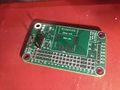
The Resulting Set of Boards
- ESP-M3 Everything!
- (The original board)
- Built AND Tested... Successfully!
- ESP-01 Everything!
- ESP-07 Everything!
- Built AND Tested... (mostly) Successfully!
- Board needs a respin...
- ESP-01F Everything!
- ESP-12 Everything!
- ESP-?? Everything!
- (The generic board)
- ESP-SoC Everything!
- (The over board)
- ESP-Everything! Programming adaptor
- ESP-Else! (Carrier boards for other bits)