Difference between revisions of "Sonoff D1"
Jump to navigation
Jump to search
(Created page with "==First Impressions== Seems pretty easy to open up. One philips screw from the front. (Needs a skinny screwdriver tho...) none|thumb First thing you se...") |
|||
| Line 1: | Line 1: | ||
==First Impressions== | ==First Impressions== | ||
Seems pretty easy to open up. One philips screw from the front. (Needs a skinny screwdriver tho...) | Seems pretty easy to open up. One philips screw from the front. (Needs a skinny screwdriver tho...) | ||
| − | [[File:Sonoff D1.jpg|none|thumb]] | + | [[File:Sonoff D1.jpg|none|thumb|link=Special:FilePath/Sonoff_D1.jpg]] |
First thing you see is the important part (From a hacking viewpoint). | First thing you see is the important part (From a hacking viewpoint). | ||
| − | [[File:Sonoff D1-Inside.jpg|none|thumb]] | + | [[File:Sonoff D1-Inside.jpg|none|thumb|link=Special:FilePath/Sonoff_D1-Inside.jpg]] |
There're actually 2 boards with a 4x2 interconnect. | There're actually 2 boards with a 4x2 interconnect. | ||
| − | [[File:Sonoff D1-2 boards.jpg|none|thumb]] | + | [[File:Sonoff D1-2 boards.jpg|none|thumb|link=Special:FilePath/Sonoff_D1-2_boards.jpg]] |
| − | [[File:Sonoff D1-between the boards.jpg|none|thumb]] | + | [[File:Sonoff D1-between the boards.jpg|none|thumb|link=Special:FilePath/Sonoff_D1-between_the_boards.jpg]] |
All the power stuff is on the one on the right. | All the power stuff is on the one on the right. | ||
| − | [[File:Sonoff D1-Power top.jpg|none|thumb]] | + | [[File:Sonoff D1-Power top.jpg|none|thumb|link=Special:FilePath/Sonoff_D1-Power_top.jpg]] |
The one on the left is the WiFi & RF board. | The one on the left is the WiFi & RF board. | ||
| − | [[File:Sonoff D1-wifi + rf top.jpg|none|thumb]] | + | [[File:Sonoff D1-wifi + rf top.jpg|none|thumb|link=Special:FilePath/Sonoff_D1-wifi_+_rf_top.jpg]] |
==Notes== | ==Notes== | ||
| Line 90: | Line 90: | ||
!Pin | !Pin | ||
!Label | !Label | ||
| + | ! | ||
! | ! | ||
! | ! | ||
| Line 97: | Line 98: | ||
| | | | ||
| | | | ||
| + | |toward edge | ||
|- | |- | ||
|2 | |2 | ||
| Line 102: | Line 104: | ||
|U3 | |U3 | ||
|5 | |5 | ||
| + | | | ||
|- | |- | ||
|3 | |3 | ||
| Line 107: | Line 110: | ||
|U3 | |U3 | ||
|6 | |6 | ||
| + | | | ||
|- | |- | ||
|4 | |4 | ||
| Line 112: | Line 116: | ||
| | | | ||
| | | | ||
| + | |toward centre | ||
|} | |} | ||
| Line 119: | Line 124: | ||
!Pin | !Pin | ||
!Label | !Label | ||
| + | ! | ||
! | ! | ||
! | ! | ||
| Line 126: | Line 132: | ||
| | | | ||
| | | | ||
| + | |toward edge | ||
|- | |- | ||
|2 | |2 | ||
| Line 131: | Line 138: | ||
|U5 | |U5 | ||
|25 | |25 | ||
| + | | | ||
|- | |- | ||
|3 | |3 | ||
| Line 136: | Line 144: | ||
|U5 | |U5 | ||
|26 | |26 | ||
| + | | | ||
|- | |- | ||
|4 | |4 | ||
| Line 141: | Line 150: | ||
| | | | ||
| | | | ||
| + | |toward centre | ||
|} | |} | ||
| Line 150: | Line 160: | ||
!Label | !Label | ||
!Connects to | !Connects to | ||
| + | ! | ||
|- | |- | ||
|GND | |GND | ||
| Line 156: | Line 167: | ||
|BUZZER | |BUZZER | ||
|U3 pin 1 | |U3 pin 1 | ||
| + | |toward centre | ||
|- | |- | ||
|GND | |GND | ||
| Line 162: | Line 174: | ||
|ZERO_CROSS | |ZERO_CROSS | ||
|U3 pin 20 | |U3 pin 20 | ||
| + | | | ||
|- | |- | ||
|GND | |GND | ||
| Line 168: | Line 181: | ||
|CONTROL | |CONTROL | ||
|U3 pin 13 | |U3 pin 13 | ||
| + | | | ||
|- | |- | ||
|3v3 | |3v3 | ||
| Line 174: | Line 188: | ||
|3v3 | |3v3 | ||
| | | | ||
| + | |toward edge | ||
|} | |} | ||
| Line 181: | Line 196: | ||
S2 is a slide switch labelled "OTA" (Not the default position...). This switch appears to be accessible through a small slot in the front cover of the unit. | S2 is a slide switch labelled "OTA" (Not the default position...). This switch appears to be accessible through a small slot in the front cover of the unit. | ||
| − | == Links == | + | ==Links== |
[https://github.com/arendst/Tasmota/issues/7598 Tasmota - Issues - #7598 - Support for Sonoff D1 Dimmer] | [https://github.com/arendst/Tasmota/issues/7598 Tasmota - Issues - #7598 - Support for Sonoff D1 Dimmer] | ||
Latest revision as of 00:21, 12 December 2022
Contents
First Impressions
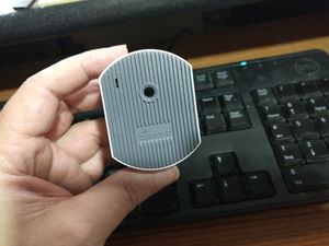
Seems pretty easy to open up. One philips screw from the front. (Needs a skinny screwdriver tho...)
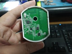
First thing you see is the important part (From a hacking viewpoint).
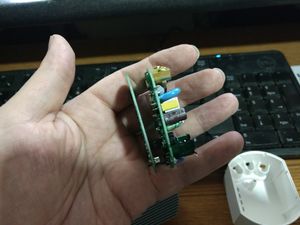
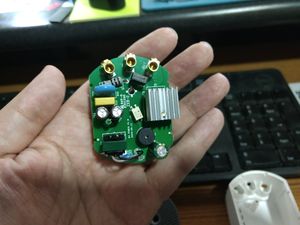
There're actually 2 boards with a 4x2 interconnect.
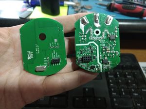
All the power stuff is on the one on the right.
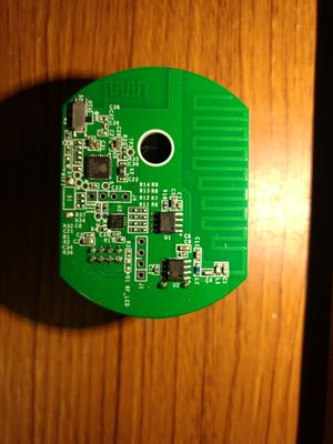
The one on the left is the WiFi & RF board.
Notes
There are 4 chips on the WiFi & RF board:
| Label | Part | Notes |
|---|---|---|
| U1 | Eastsoft ES7P001FGSA GS34BFN404 | 8-bit MCU? |
| U2 | 590R 1933 | Probably the RF chip |
| U3 | BB10 F8G A01J1J 1939 A | 8-bit MCU |
| U5 | ESP8285 |
There are 7 test points immediately accessible on the board:
| Label | Signal | ESP
Pin |
Notes |
|---|---|---|---|
| TP3 | EXT_RSTB | 32 | Possibly useful for reset when flashing? |
| 5 | GPIO5 | 24 | |
| 4 | GPIO4 | 16 | |
| 0 | GPIO0 | 16 | |
| 6 | GPIO2 | 14 | |
| RX | UORXD | 25 | Also connected to U3 pin 17 via 0Ω resistor R16 |
| TX | UORXD | 26 | Also connected to U3 pin 18 via 0Ω resistor R15 |
This board has 2 4-pin header locations.
J1 seems to connect to U3.
| Pin | Label | |||
|---|---|---|---|---|
| 1 | 3v3 | toward edge | ||
| 2 | C2CK | U3 | 5 | |
| 3 | C2D | U3 | 6 | |
| 4 | GND | toward centre |
J4 connexts to RX & TX on the ESP chip.
| Pin | Label | |||
|---|---|---|---|---|
| 1 | 3v3 | toward edge | ||
| 2 | E-RX | U5 | 25 | |
| 3 | E-TX | U5 | 26 | |
| 4 | GND | toward centre |
The interconnect to the power board:
| Label | Pin # | Label | Connects to | ||
|---|---|---|---|---|---|
| GND | 1 | BUZZER | U3 pin 1 | toward centre | |
| GND | ZERO_CROSS | U3 pin 20 | |||
| GND | CONTROL | U3 pin 13 | |||
| 3v3 | 3v3 | toward edge | |||
There are 2 switch locations on the board.
S1 is un-populated but seems to be for a push-button on the ESP chips GPIO0 pin.
S2 is a slide switch labelled "OTA" (Not the default position...). This switch appears to be accessible through a small slot in the front cover of the unit.
